
Growth and characterization of planar hexagonal Ge on CdS
Source: arXiv:2607.24685 · Published 2026-07-27 · By Andrea Besana, Veronica Regazzoni, Marco Faverzani, Fabrizio Rovaris, Emiliano Bonera, Sonia Freddi et al.
TL;DR
This paper addresses the challenge of epitaxially growing and stabilizing planar hexagonal germanium (Ge-2H), a metastable allotrope with promising electronic and optical properties distinct from conventional cubic Ge. The authors demonstrate the epitaxial growth of planar hexagonal Ge films on non-basal m-plane CdS substrates using low-energy plasma-enhanced chemical vapor deposition (LEPECVD), focusing on optimizing growth temperature to stabilize the hexagonal phase. Detailed structural, morphological, and optical characterizations—including X-ray diffraction (XRD), scanning transmission electron microscopy (STEM), polarization-resolved Raman spectroscopy, and photoluminescence (PL)—confirm the formation of epitaxial Ge-2H with characteristic lattice parameters and phonon modes. Defect analysis combined with atomistic modeling reveals that strain relaxation occurs primarily within a few nanometers of the interface via a limited set of dislocation mechanisms that include localized cubic stacking faults, and that stacking-fault disorder dominates further from the interface causing gradual loss of hexagonal order. These findings establish CdS (1¯100) as a promising planar template for hexagonal Ge and provide insight into strain relaxation and defect formation in metastable group-IV heterostructures, potentially enabling future integration of Ge-2H in planar device architectures.
Key findings
- Epitaxial growth of planar hexagonal Ge achieved on non-basal (1¯100) CdS substrates at optimized growth temperature of ~250 °C via LEPECVD.
- Above 300 °C growth leads to thermochemical degradation and Ge–CdS intermixing with mushroom-like aggregates, limiting practical growth temperature.
- At 200 °C, Ge layers form as continuous but amorphous films due to low adatom mobility; crystalline hexagonal phase forms only at intermediate temperatures.
- XRD shows hexagonal Ge lattice parameters a⊥ ≈ 0.3999 nm and c ≈ 0.664 nm, close but slightly different from nanowire-grown Ge-2H, with ~2:1 ratio hexagonal-to-cubic phase volume estimated from peak intensities.
- Polarized Raman spectroscopy confirms characteristic E2g phonon mode of hexagonal Ge with polarization selection rules matching 2H symmetry, at ~287–290 cm-1 peak position.
- Photoluminescence measurements do not detect Ge-related emission, likely due to weak pseudo-direct bandgap emission and limited layer thickness.
- STEM and atomistic modeling reveal strain relaxation within first ~5 nm from interface via dislocations causing localized cubic stacking insertions; beyond ~12 nm, stacking faults (I3-type) dominate and degrade hexagonal order.
- Layer morphology and structural quality maintained up to 50 nm thickness, but hexagonal phase purity decreases with thickness due to increasing stacking disorder.
Methodology — deep read
The authors start with the threat and challenge of stabilizing metastable hexagonal germanium in planar heterostructures, assuming the main barrier is kinetic control over the stacking sequence and strain from lattice mismatch.
Their data comprises germanium layers grown on commercially obtained single-crystal CdS (1¯100) wafers using a LEPECVD system. Germane (GeH4) was the precursor gas, and growth temperatures ranged from 200 to 300 °C with deposition rates near 0.05 nm/s. Four samples with various thicknesses (10–50 nm) and growth temperatures (200, 250, 300 °C) were prepared. Substrates were cleaned chemically then heated to temperature in vacuum before deposition.
Extensive characterization was conducted: atomic force microscopy (AFM) and scanning electron microscopy (SEM) to assess surface morphology; cross-sectional scanning transmission electron microscopy (STEM) with electron energy loss spectroscopy (EELS) and energy dispersive X-ray spectroscopy (EDX) for atomic structure and composition at the interface; high-resolution X-ray diffraction (HR-XRD) for lattice parameters and phase identification; polarized Raman spectroscopy to probe phonon modes and crystal symmetry; low-temperature photoluminescence to detect optical emission. STEM samples were prepared by focused ion beam milling.
XRD reciprocal space mapping identified hexagonal phase peaks and allowed quantification of lattice constants and phase fractions by comparing with CdS substrate reflections and cubic Ge references. Polarized Raman spectra were recorded with backscattering geometry, rotating sample orientation to confirm the expected selection rules for hexagonal E2g phonon modes.
STEM imaging along specific zone axes identified stacking sequences and localized defects. Atomistic modeling and molecular dynamics simulations complemented TEM data to explain dislocation types and strain relief mechanisms, including partial dislocations causing cubic stacking faults and a-type dislocations relieving strain along orthogonal directions.
This systematic multitechnique approach allowed correlation of growth conditions with phase formation, morphology, strain relaxation mechanisms, and optical signatures, providing a comprehensive picture of the formation and stability of planar Ge-2H films on CdS.
End-to-end example: at 250 °C and 10 nm thickness, cross-sectional STEM imaging clearly shows ABAB hexagonal stacking with some cubic inclusions near the interface, consistent with XRD detection of dominant hexagonal peaks. Polarized Raman confirms E2g mode with correct polarization dependence, while PL fails to detect Ge emission. STEM and modeling identify strain-accommodating dislocations introducing cubic stacking faults within a few nanometers, explaining initial strain relaxation, while stacking faults increase with thickness degrading 2H order.
Technical innovations
- Demonstrated low-energy plasma-enhanced CVD growth of planar hexagonal Ge on non-basal m-plane CdS substrates, enabling planar heteroepitaxy of metastable Ge-2H.
- Detailed correlation of growth temperature with phase formation, showing narrow optimal window (~250 °C) to avoid amorphous or thermochemically degraded layers.
- Use of polarized Raman spectroscopy to unambiguously confirm hexagonal Ge crystal symmetry via characteristic E2g phonon polarization selection rules.
- Combined atomic-resolution STEM observations with atomistic modeling to identify specific dislocation types responsible for anisotropic strain relaxation in Ge-2H layers.
- Quantitative phase fraction estimation of coexisting hexagonal and cubic domains via reciprocal space mapping using XRD, linking defect formation to partial cubic stacking insertions.
Datasets
- Sample I: 30 nm Ge on CdS at 300 °C
- Sample II: 50 nm Ge on CdS at 200 °C
- Sample III: 10 nm Ge on CdS at 250 °C
- Sample IV: 50 nm Ge on CdS at 250 °C
Baselines vs proposed
- Growth at 300 °C: formation of dendritic mushroom-like structures with strong Ge–CdS intermixing vs 250 °C: uniform epitaxial hexagonal Ge layer formation
- Growth at 200 °C: amorphous Ge films with Raman amorphous peak only vs 250 °C: clear hexagonal Ge Raman modes and XRD peaks
- XRD: hexagonal to cubic Ge phase volume roughly 2:1 ratio, demonstrating majority hexagonal phase in optimal samples
Figures from the paper
Figures are reproduced from the source paper for academic discussion. Original copyright: the paper authors. See arXiv:2607.24685.
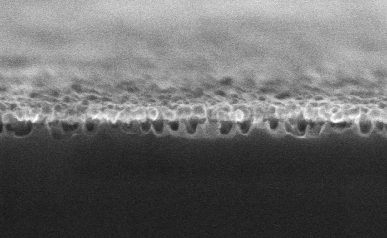
Fig 1: Growth-temperature dependence of the morphological properties of Ge/CdS samples. (a) In-plane and (b) cross-
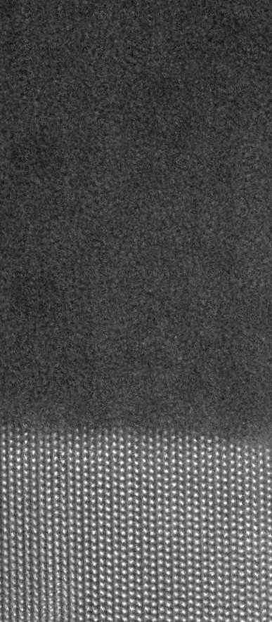
Fig 2: Cross-sectional HAADF-STEM image of sample IV (a 50 nm-thick Ge layer, Tg ≈250 °C) obtained along the (a)
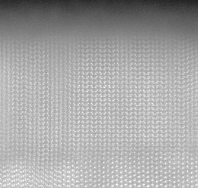
Fig 3: High-resolution X-ray diffraction reciprocal space maps for sample IV around the (a) (2¯201) and (b) (2¯310) Bragg
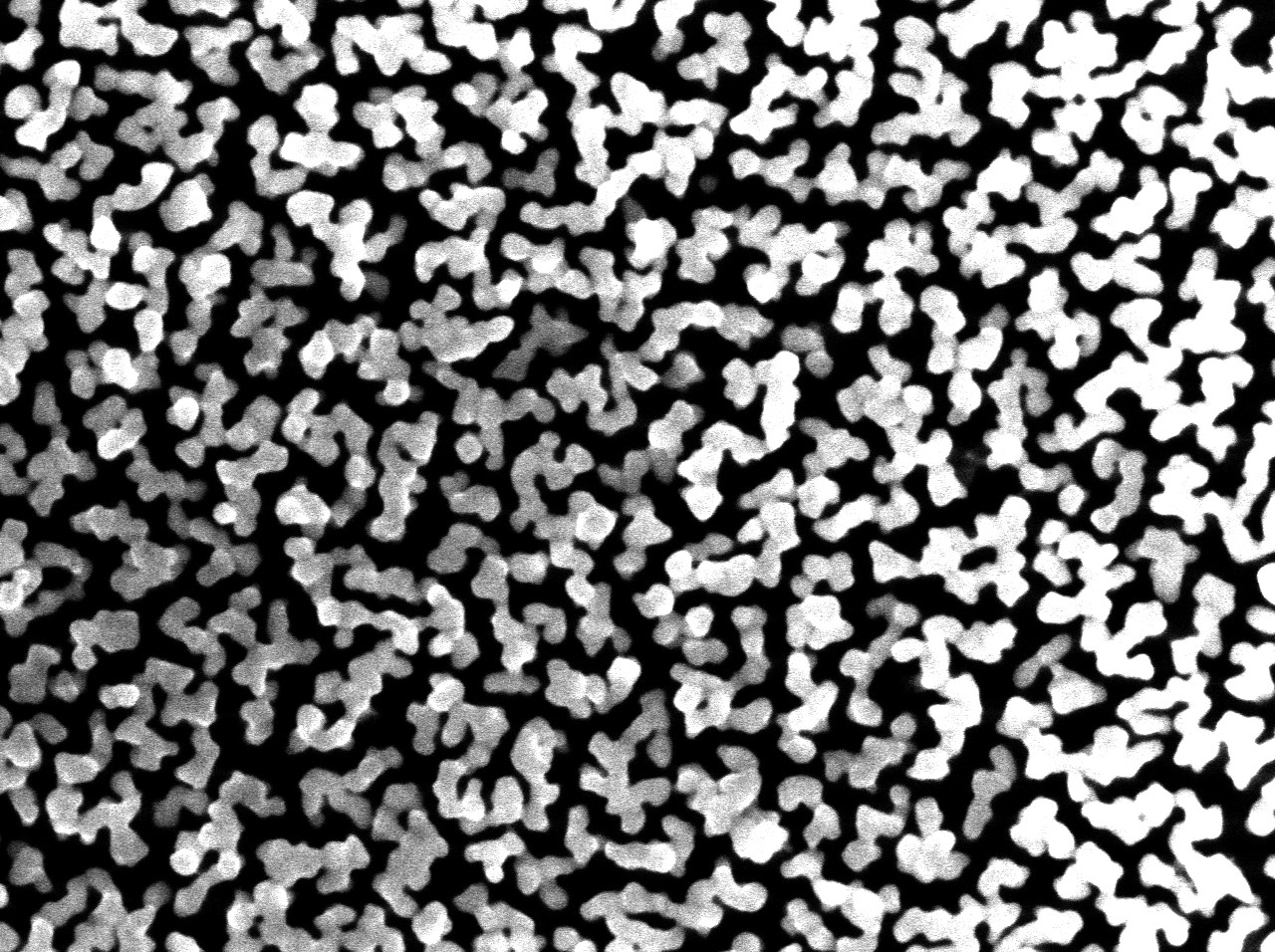
Fig 5: shows the PL spectra of sample IV (50 nm-
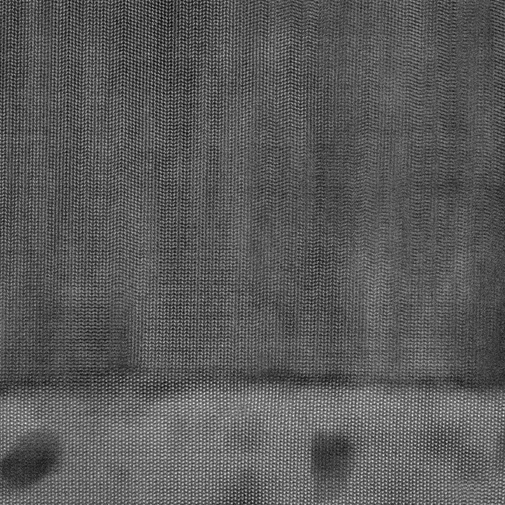
Fig 4: Polarization-resolved Raman spectra of Ge/CdS. (a)
Fig 6 (page 5).
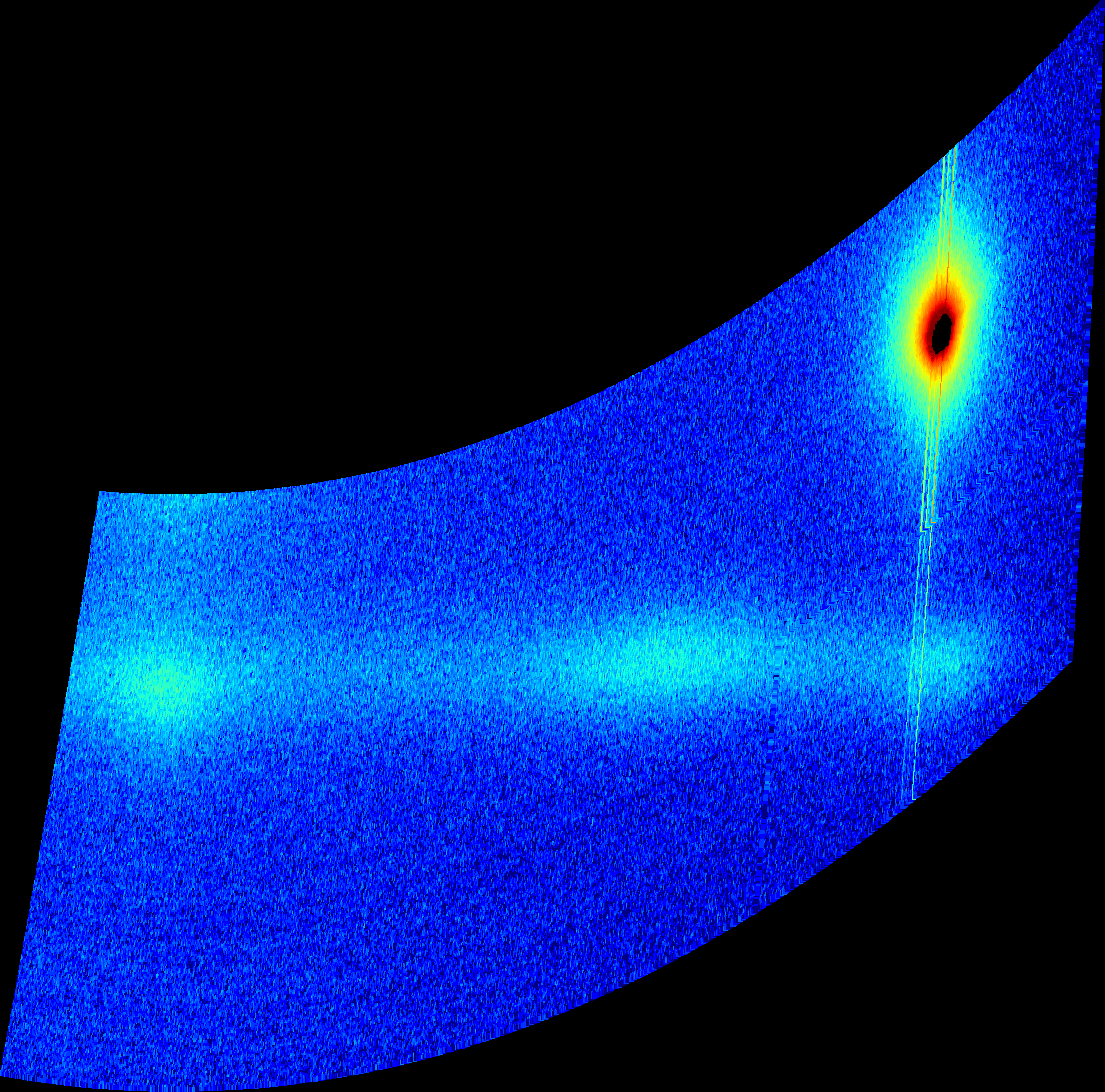
Fig 7 (page 5).
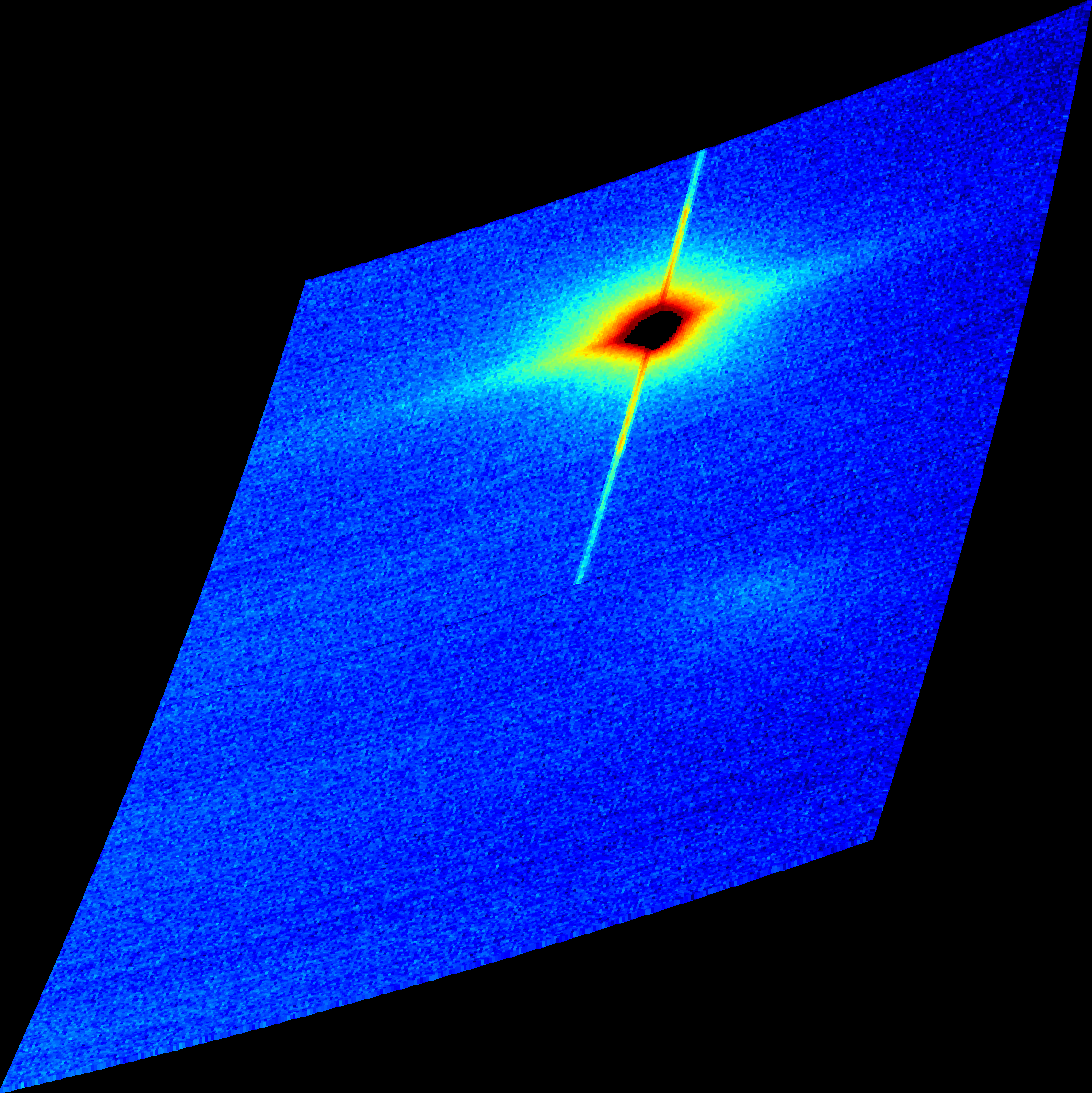
Fig 8 (page 5).
Limitations
- Photoluminescence measurements did not detect Ge-related emission, limiting optical confirmation of bandgap properties.
- Hexagonal phase purity degrades significantly beyond tens of nanometers due to stacking fault accumulation, indicating limited thickness scalability.
- Growth temperature window is narrow; above 300 °C, thermochemical degradation occurs, imposing practical constraints.
- Analysis focuses on static structural and optical characterization; no direct device demonstration or electrical property measurement.
- Atomistic modeling limited to defect types observed experimentally; additional unobserved defect mechanisms may exist.
Open questions / follow-ons
- Can thicker Ge-2H layers with preserved hexagonal purity be grown by alternative strain management or substrate engineering?
- What are the detailed electronic and spin properties of planar Ge-2H films, especially regarding direct bandgap and spin manipulation capabilities?
- How do the identified interfacial dislocations and stacking faults affect carrier transport and optical recombination in Ge-2H?
- Can growth methods be optimized to suppress cubic stacking insertions and stacking faults further?
Why it matters for bot defense
While not directly related to bot defense or CAPTCHA design, this work illustrates rigorous experimental and modeling methodology for stabilizing novel metastable semiconductor phases in planar heterostructures. Bot-defense researchers focusing on integrating photonic or spintronic devices based on new semiconductor materials could find the insights on strain relaxation and phase stability useful. Understanding defect formation and impact on optical properties may inform design of robust optical sources or photodetectors used in biometric CAPTCHA systems or anti-bot sensors. The combination of multiscale microscopy, spectroscopy, and atomistic simulation exemplifies a comprehensive approach to novel material characterization, relevant for advanced optical and sensing system development in security applications.
Cite
@article{arxiv2607_24685,
  title={ Growth and characterization of planar hexagonal Ge on CdS },
  author={ Andrea Besana and Veronica Regazzoni and Marco Faverzani and Fabrizio Rovaris and Emiliano Bonera and Sonia Freddi and Elisa Brugaletta and Mohamed Zaghloul and Fabio Pezzoli and Francesco Montalenti and Monica Bollani and Daniel Chrastina and Anna Marzegalli and Antonio M. Mio and Emilio Scalise and Giovanni Isella },
  journal={arXiv preprint arXiv:2607.24685},
  year={ 2026 },
  url={https://arxiv.org/abs/2607.24685}
}