
Direct writing of individual quantum dots
Source: arXiv:2607.11864 · Published 2026-07-13 · By Weikun Zhu, Natalie Ngoh, Shelly Ben-David, Maxwell Conte, Teddy Hsieh, Sarah O. Spector et al.
TL;DR
This paper addresses a critical challenge in scalable quantum photonic technologies: deterministic, site-selective integration of individual high-quality quantum emitters. The authors introduce a novel thermal scanning probe lithography method that enables direct synthesis ("direct writing") of inorganic halide perovskite quantum dots (QDs) at predetermined locations with sub-25 nm spatial precision. Unlike traditional stochastic dispersion of colloidal QDs or limited-resolution laser patterning, their nanoscale localized thermal growth promotes the formation of single quantum emitters in a polymeric precursor matrix. This approach achieves deterministic arrays of room-temperature, high-purity CsPbI3 single-photon emitters, comparable in optical quality to state-of-the-art colloidal alternatives but with vastly improved integration control.
Key results include high-yield (>85%) arrays of QDs with narrow linewidths (~67 meV), room-temperature single-photon purity up to 98% (g^{2}(0) as low as 0.04), and on-demand integration into photonic cavities resulting in ~3-fold enhancement of spontaneous emission rate. The technique overcomes longstanding material compatibility and resolution barriers faced by top-down fabrication, bridging the gap between chemical synthesis precision and photonic system integration. This direct-write platform thus represents a significant advancement toward scalable, functional quantum light sources for computing, communication, and sensing.
Key findings
- Achieved site-selective growth of CsPbI3 quantum dots with spatial control better than 25 nm using a thermal scanning probe technique.
- Produced arrays with >85% yield of optically active single-emitter quantum dots in a 25 nm-thick PMMA matrix containing 10.3 wt% precursors.
- Individual emitters exhibited photoluminescence peak centered at 645.3 ± 13.9 nm, linewidth of 92.3 ± 21.7 meV, and lifetime of 11.0 ± 2.7 ns, matching colloidal QD benchmarks.
- Single-photon purity confirmed with g^{2}(0) values averaging 0.12 ± 0.11 across 65 sites, with best values reaching 0.04 (98% purity) at room temperature.
- Thermal profile simulations indicate a highly localized heat zone (~110-140 °C) at the polymer glass transition, confining quantum dot nucleation to nanoscale volumes.
- Systematic tuning of precursor concentration, film thickness, and probe temperature optimized growth of individual QDs; higher precursor loading and thicker films increased multi-emitter formation (higher g^{2}(0)).
- Demonstrated deterministic integration by placing QDs with <25 nm precision at the centers of TiO2 circular Bragg grating cavities.
- Coupling to cavities enhanced spontaneous emission rate ~3-fold (reduced PL lifetime from 11 ns to 3.7 ns) without degrading single-photon purity (g^{2}(0)=0.04).
Methodology — deep read
Threat Model & Assumptions: The authors seek to fabricate deterministic single-photon emitters from inorganic perovskite QDs that can be integrated precisely with photonic structures. The key challenge is the stochastic dispersion of colloidal QDs and material incompatibilities preventing precise top-down fabrication. The adversary or failure modes here are uncontrolled emitter placement and poor emitter stability. This is a materials and fabrication engineering challenge rather than an adversarial security model.
Data: The experimental data comprises optical characterization of arrays of direct-write QDs grown in precursor polymer films on SiO2-on-Si substrates. Typical samples have 25 nm-thick PMMA films with 10.3 wt% precursors (CsX, PbX2, X=Cl,Br,I). Hundreds of individual QD sites were characterized via photoluminescence (PL) spectroscopy, lifetime, and second-order correlation measurements (g^{2}(0)) to confirm single-photon emission. Additional structural characterization used TEM and XRD to verify crystallinity and size (~4.5 nm diameter dots).
Architecture/Algorithm: The core fabrication method uses a thermal scanning probe lithography system with a silicon tip (~5 nm radius) heated to ~850 °C. The heated tip indents ~15 nm into the precursor polymer matrix, locally raising temperature to the polymer glass transition (~110-140 °C). This confined thermal volume mobilizes precursor ions within the polymer (PMMA or PMMA:PVDF blends), inducing site-selective nucleation and growth of CsPbI3 QDs directly on the substrate. This bottom-up chemical synthesis localized by additive manufacturing is novel, overcoming diffraction-limited laser patterning and top-down incompatibility.
Training Regime: Not applicable as this is an experimental materials synthesis study. Optimization was performed by varying process parameters - precursor concentration, film thickness, and probe temperature - followed by optical characterization to tune growth conditions for single QD formation.
Evaluation Protocol: Optical performance of QDs was quantified by PL spectra (peak wavelength, linewidth), time-resolved PL lifetime, and Hanbury Brown–Twiss (HBT) photon correlation measurements for g^{2}(0). Single-photon criteria require g^{2}(0)<0.5. Device yield was determined by counting optically active sites. Deterministic placement accuracy was statistically assessed across >60 samples via scanning PL maps relative to cavity centers. Cavity coupling was evaluated by comparing PL lifetimes and spectra before and after integration.
Reproducibility: The paper provides extensive experimental detail and supplementary notes on process parameters, optical setups, and characterization methods. No public code or datasets are relevant. Structural and optical characterization techniques (TEM, XRD, PL, HBT) follow standard protocols. Data supporting the findings are included or available upon reasonable request. While the precursor formulations and thermal probe parameters are clearly described, reproducing nanoscale thermal lithography may require specialized instrumentation.
Concrete Example End-to-End: A 25 nm thick PMMA film doped with 10.3 wt% CsPbI3 precursors is spin-coated onto a SiO2-on-Si substrate. A silicon thermal probe tip of 5 nm radius, heated to 850 °C and indented 15 nm into the film, locally raises temperature to ~130 °C near the tip, causing precursor ions to become mobile and nucleate growth of a ~4.5 nm CsPbI3 quantum dot exactly beneath the tip. Photoluminescence measurements reveal a sharp emission peak at ~665 nm with 67 meV linewidth and a PL lifetime of 13 ns. Single-photon emission is confirmed by g^{2}(0)=0.04 in photon correlation, indicative of a single quantum emitter. By repeating this with precise tip scanning, arrays of single QDs are formed with <25 nm placement accuracy. Integration of such QDs into TiO2 circular Bragg grating cavities enhances spontaneous emission rate ~3-fold without loss of single-photon purity.
Technical innovations
- Use of thermal scanning probe lithography to create a nanoscale localized thermal volume inducing site-selective in-situ synthesis of halide perovskite quantum dots with individual-emitter resolution.
- Engineering of precursor-polymer matrices with tunable glass transition temperatures to confine quantum dot nucleation spatially and thermally.
- Demonstration of deterministic placement and synthesis of single perovskite QDs with <25 nm spatial precision enabling direct integration with photonic cavities.
- Integration of bottom-up atomic-scale chemical synthesis precision with additive manufacturing spatial control to overcome diffraction and material compatibility limitations of prior top-down and laser patterning techniques.
Datasets
- Direct-write CsPbI3 quantum dots arrays — 65+ emitters characterized optically — experimental samples fabricated on SiO2-on-Si substrates
Baselines vs proposed
- Colloidal CsPbI3 quantum dots: single-photon purity (g^{2}(0)) ~0.04 reported in literature (refs 24-26) vs direct-write QDs: g^{2}(0) average 0.12 ± 0.11, best 0.04
- Colloidal CsPbI3 QDs: PL linewidth ~67-90 meV vs direct-write emitters: 67-92 meV
- Lifetime on planar substrate: 11.0 ± 2.7 ns vs cavity-coupled direct-write QDs: 3.7 ns (3x spontaneous emission enhancement)
- Optically active yield for solution-deposited QDs: random dispersion vs >85% yield for direct-written QDs
Figures from the paper
Figures are reproduced from the source paper for academic discussion. Original copyright: the paper authors. See arXiv:2607.11864.
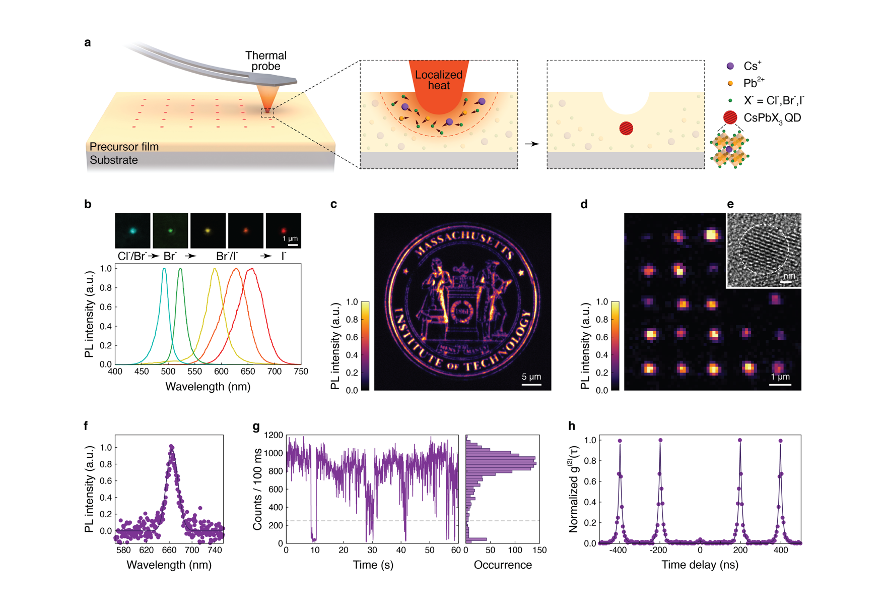
Fig 1: | Direct writing of perovskite QDs with single-emitter resolution. a, Schematic
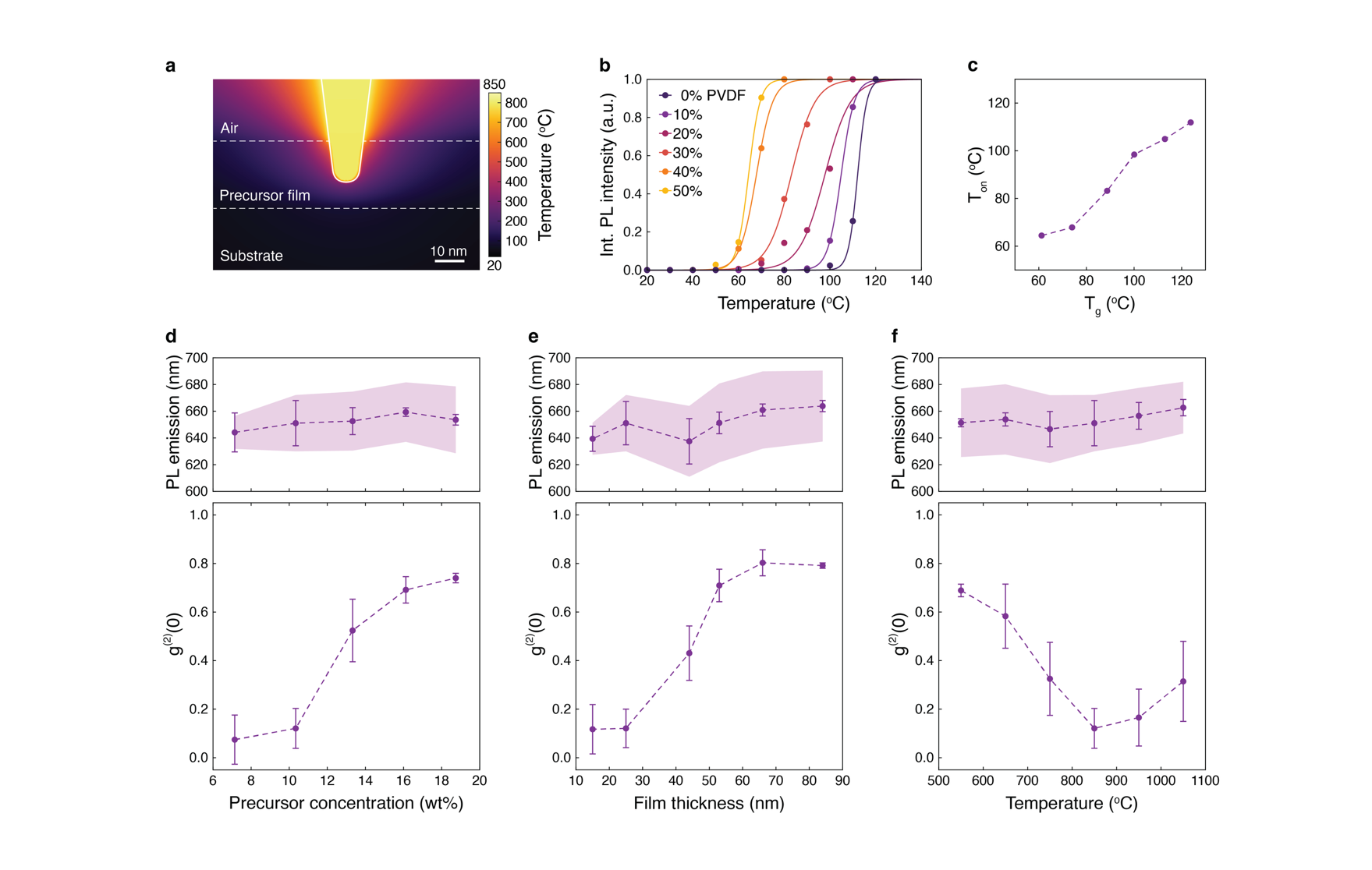
Fig 2: | Direct writing optimization for single-photon emitters. a, Simulated thermal profile of
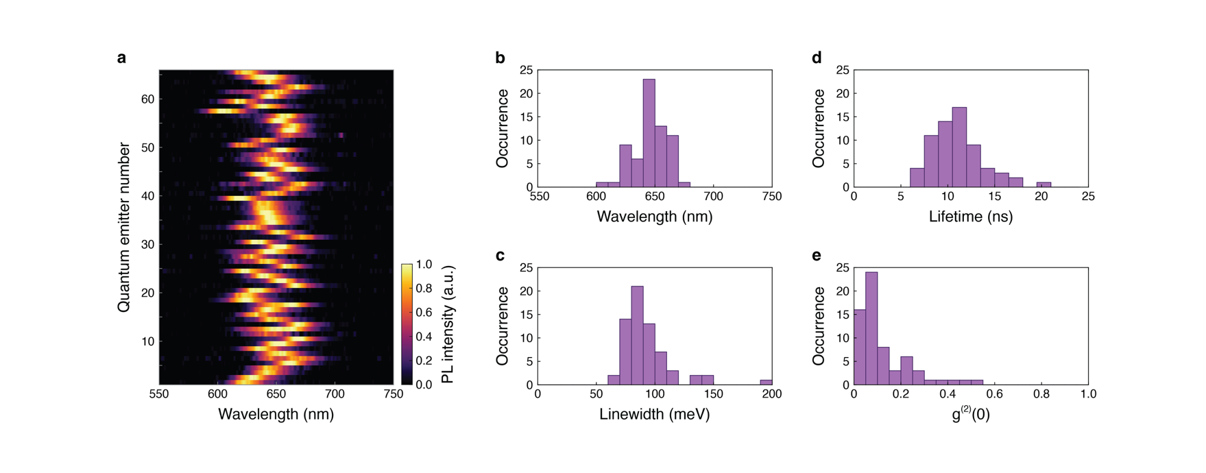
Fig 3: | Optical characteristics of direct-write CsPbI3 single-photon emitters. a, PL spectra of
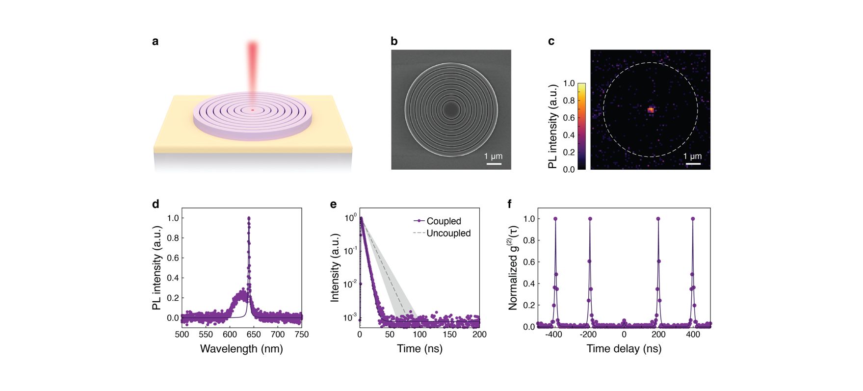
Fig 4: | Deterministic coupling of the direct-write QDs to photonic cavities. a, Schematic of a
Limitations
- Thermal scanning probe lithography requires specialized, potentially low-throughput instrumentation limiting scale.
- Quantum dot synthesis parameters are tightly constrained; precursor concentration, polymer film thickness, and temperature require optimization that may differ for other material systems.
- Only CsPbI3 perovskite QDs and PMMA-based matrices were demonstrated; generality to other materials or substrates is untested.
- Single-photon purity and brightness stability characterization were conducted at room temperature but long-term photostability under operating conditions was not extensively reported.
- The paper does not demonstrate integration in complex circuit architectures or devices beyond single cavity coupling.
- No adversarial robustness or device reliability analyses under environmental variation were presented.
Open questions / follow-ons
- Can this direct-write approach be applied to other quantum emitter materials and heterostructures beyond CsPbI3 perovskite QDs?
- How scalable and repeatable is the thermal scanning probe lithography process for large-area device fabrication and integrated quantum photonic circuits?
- What are the long-term stability and photobleaching characteristics of the direct-written QDs under continuous operation in different environments?
- Can the approach enable multi-emitter arrays with engineered emitter-emitter interactions for complex quantum networks?
Why it matters for bot defense
While this paper is primarily focused on quantum photonic emitter fabrication rather than bot-defense or CAPTCHA technologies, the demonstrated deterministic nanofabrication approach exemplifies how precise spatial and material control at the nanoscale enables on-demand creation of functional quantum light sources. Bot-defense systems that rely on physical unclonable functions or optical device verification could benefit from emerging classes of integrated quantum emitters offering unique optical fingerprints. Moreover, the ground-truth ability to place single-photon sources exactly at photonic structures could guide novel optical challenge-response schemes in CAPTCHA systems harnessing non-classical light. The additive manufacturing strategy combining bottom-up synthesis and atomic-scale spatial control sets an important precedent for future quantum-enabled security device engineering, though direct application to CAPTCHA tasks has yet to be explored.
Cite
@article{arxiv2607_11864,
  title={ Direct writing of individual quantum dots },
  author={ Weikun Zhu and Natalie Ngoh and Shelly Ben-David and Maxwell Conte and Teddy Hsieh and Sarah O. Spector and Tara Sverko and Patricia Jastrzebska-Perfect and Will Jack and Jinwoo Sim and Peter F. Satterthwaite and Farnaz Niroui },
  journal={arXiv preprint arXiv:2607.11864},
  year={ 2026 },
  url={https://arxiv.org/abs/2607.11864}
}