
Nanoelectromechanical Systems (NEMS) for Hardware Security in Advanced Packaging
Source: arXiv:2606.26426 · Published 2026-06-24 · By Himanandhan Reddy Kottur, Pavanbabu Arjunamahanthi, M. Shafkat M. Khan, Liton Kumar Biswas, Nitin Varshney, Navid Asadizanjani
TL;DR
This paper addresses the escalating hardware security challenges in semiconductor manufacturing and advanced packaging by proposing Nanoelectromechanical Systems (NEMS) as novel hardware security primitives. Traditional electronic security measures such as cryptographic keys and electronic PUFs suffer from vulnerabilities to side-channel attacks, aging, and reverse engineering; NEMS provide a fundamentally different security modality based on nanoscale mechanical unpredictability and fabrication-induced physical variations. The authors survey key NEMS-based mechanisms including NEMS-PUFs, shape memory materials for tamper detection, resonance-based fingerprints for authentication, and physical locking/unlocking architectures embedded within semiconductor packages. These technologies offer inherent tamper evidence, high entropy unclonable signatures, low power operation, and compatibility with standard CMOS process flows, enabling scalable solutions across defense, aerospace, critical infrastructure, and consumer electronics. However, integration and reliability challenges remain due to the extreme sensitivity of NEMS devices during packaging.
Key findings
- NEMS-PUFs leverage nanoscale mechanical and structural irregularities to produce physically unclonable functions with high entropy and resistance to invasive attacks like FIB and microprobing.
- Shape memory alloys and polymers integrated into NEMS provide irreversible, power-independent tamper-evident responses triggered by temperature or mechanical stress.
- Resonance-based NEMS fingerprints produce unique, physically rooted identifiers from resonance frequency variations due to fabrication imperfections, enabling low-power, highly secure authentication.
- NEMS-enabled locking/unlocking mechanisms embedded in redistribution layers enable controlled chip activation based on external stimuli, mitigating unauthorized use and reverse engineering.
- NEMS devices’ nanoscale dimensions (under 100 nm) make them highly sensitive to mechanical, thermal, and chemical stress during packaging steps such as die attach and reflow, impacting yield and reliability.
- Standard OSAT workflows require costly adaptations like low-damage encapsulation and particle-free handling to preserve NEMS structural and functional integrity.
- Integration challenges include managing coefficient of thermal expansion mismatch and electromagnetic interference to maintain NEMS performance and authentication accuracy.
- The paper highlights the scalability potential of NEMS since they are CMOS compatible and can integrate with advanced packaging without added security ICs, reducing complexity and cost.
Threat model
The adversary is a sophisticated entity capable of physical tampering with semiconductor devices post-fabrication via invasive techniques such as focused ion beam editing, laser fault injection, microprobing, and reverse engineering to extract keys, clone devices, or insert malicious modifications. They lack the ability to perfectly replicate inherent nanoscale mechanical variations underlying NEMS structures without destructively altering their signatures. The adversary may observe communications and attempt side-channel analysis but cannot infinitely simulate or reset irreversible physical tampering responses embedded within shape memory materials or NEMS-PUFs.
Methodology — deep read
The authors begin by defining the threat model: adversaries can physically tamper with semiconductor devices at various stages including packaging and supply chain, using advanced invasive techniques like laser fault injection, focused ion beam editing, and microprobing. The attackers attempt to extract keys, clone devices, or insert backdoors, but cannot easily replicate nanoscale physical structures without corrupting their integrity. The study synthesizes research on several NEMS security primitives rather than reporting new datasets or models. Key data reviewed includes the nanoscale variability intrinsic to fabricated NEMS structures, shape memory material phase transitions, resonance frequency measurements from resonators, and integration challenges from packaging literature. For NEMS-PUFs, fabrication-induced variations (surface roughness, grain boundaries, mechanical stiffness) create unique mechanical responses recorded as physical fingerprints. The review discusses the use of stiction effects caused by van der Waals forces in nanowires as entropy sources for PUFs. Shape memory alloys (SMA) and polymers (SMP) enable irreversible and reversible tamper responses triggered by environmental stimuli such as heat or mechanical force; these responses produce permanent physical signatures independent of power or software logs. Resonator-based fingerprints leverage resonance frequency deviations from fabrication imperfections to authenticate devices passively at ultra-low power. The paper details locking/unlocking mechanisms integrated within semiconductor device redistribution layers (RDLs) that respond to specific physical triggers (temperature, electrical signals) to activate or lock device functionalities, preventing unauthorized use. Challenges analyzing NEMS integration include detecting material fatigue, stiction, CTE-induced stress, moisture ingress, and electromagnetic interference impacting device reliability and PUF entropy. Mitigation methods include low-temperature bonding, particle-free clean-room conditions, hermetic encapsulation, and electromagnetic shielding. Evaluation protocols referenced include comparing entropy and tamper resistance metrics of NEMS-PUFs vs electronic PUFs, demonstration of irreversible shape changes under tampering for shape memory materials, and resonance uniqueness measured via frequency spectra. The paper references prior experimental studies for some metrics but does not provide new empirical results or code releases. One representative end-to-end example is the embedding of NEMS resonators into packaging layers that generate unique resonance responses unaffected by electromagnetic side-channel attacks and can detect tampering via frequency shifts induced by physical damage.
Technical innovations
- Application of nanoscale mechanical variability in NEMS as an entropy source for physically unclonable functions, advancing beyond electronic PUFs sensitive to environmental degradation.
- Integration of shape memory materials into packaging layers for irreversible, passive tamper-evident mechanisms that do not depend on power or digital logs.
- Use of resonance frequency fingerprints from NEMS resonators as low-power, physically rooted hardware identifiers resistant to duplication and side-channel attacks.
- Development of NEMS-based locking/unlocking architectures embedded in device packaging, enabling controlled activation triggered by physical stimuli to prevent unauthorized access.
Baselines vs proposed
- Electronic PUFs: reliability degrades over time with thermal/electrical stress versus NEMS-PUFs showing higher stability under environmental variation (referenced but no numerical metrics provided).
- Conventional circuits prone to microprobing attacks (left in Fig 3) versus NEMS-resonator-enhanced designs offering improved mechanical fingerprinting and tamper resilience (right in Fig 3).
Figures from the paper
Figures are reproduced from the source paper for academic discussion. Original copyright: the paper authors. See arXiv:2606.26426.
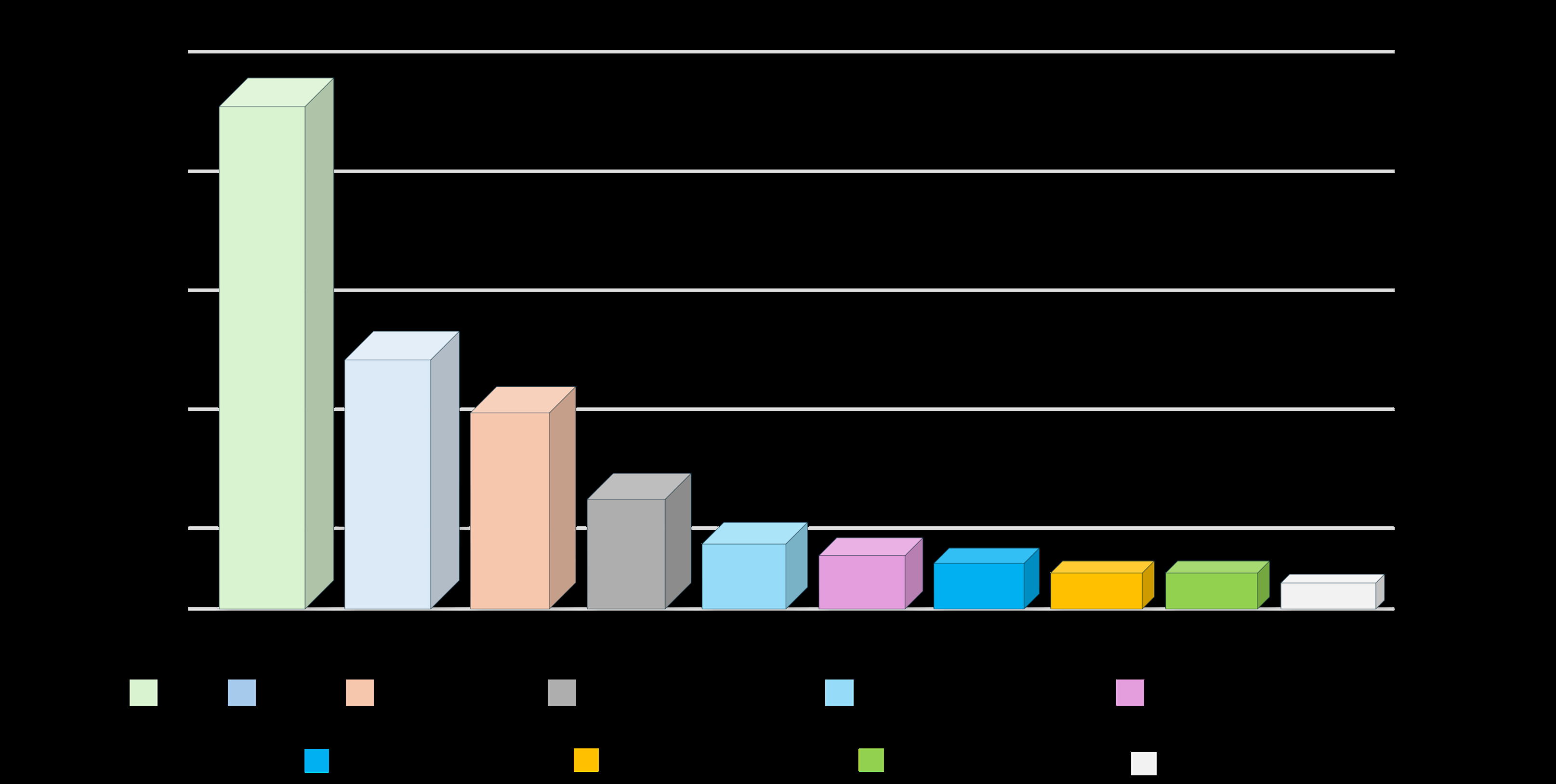
Fig 1: Global revenue (in millions USD) of major advanced packaging OSATs companies [14]
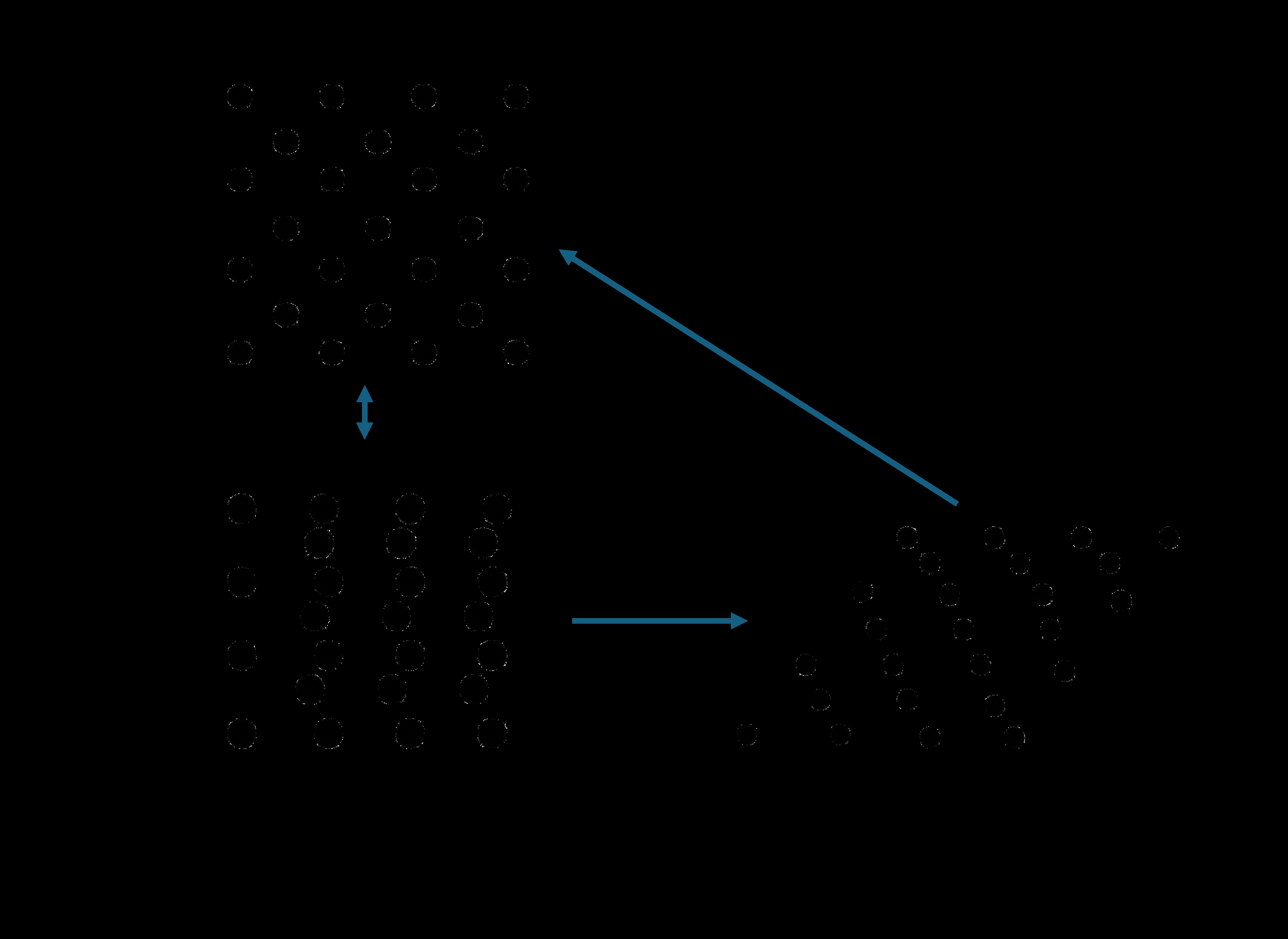
Fig 2: Microstructural views of martensite and austenite
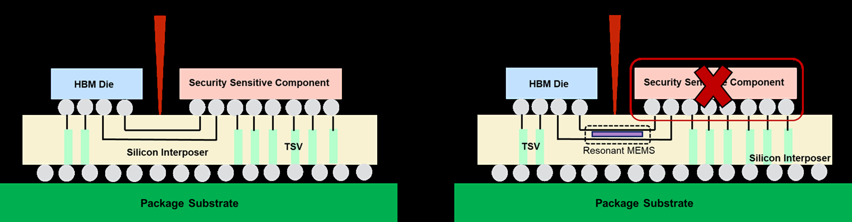
Fig 3: Conventional circuit prone to Microprobing (left) versus NEMS-resonator-enhanced design offering mechanical
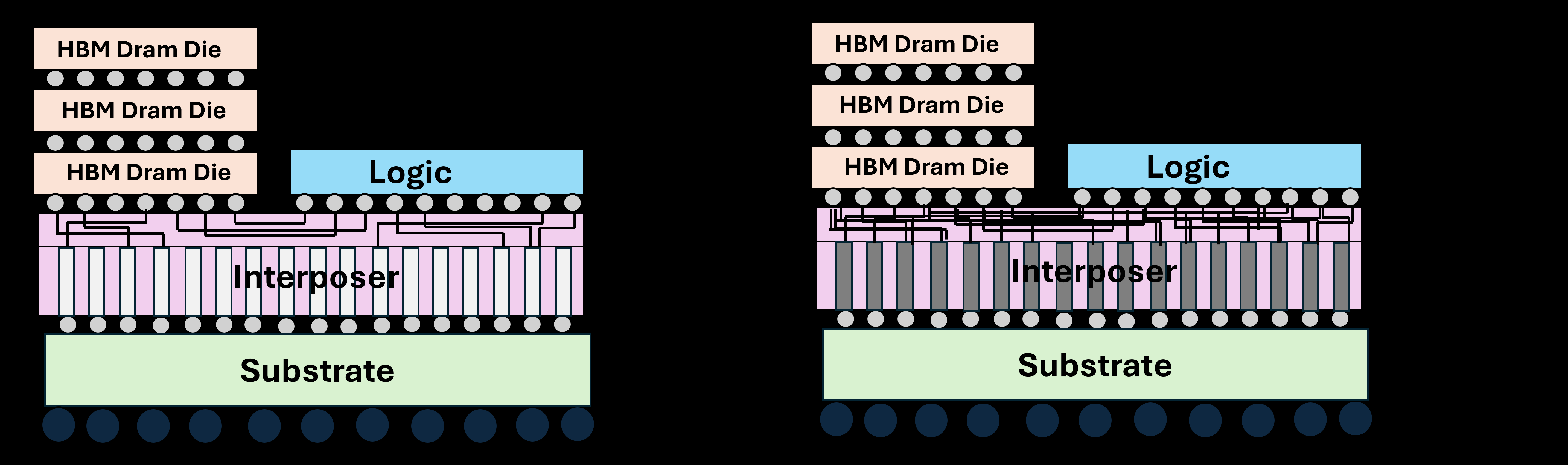
Fig 4: Illustration of locking/unlocking mechanisms using NEMS integrated into the redistribution layer (RDL) [28]. These
Limitations
- No new experimental data or quantitative results are provided; results are summarized from literature and prior studies.
- Integration challenges such as mechanical damage during packaging and susceptibility to environmental noise limit current scalability of widespread NEMS deployment.
- Costly manufacturing process adaptations are required for damage mitigation, impacting high-volume production feasibility.
- Lack of evaluation under active adversarial attack scenarios or long-term aging studies reduces maturity of security claims.
- Unclear how NEMS-PUFs perform under extreme environmental conditions or in presence of advanced side-channel analysis beyond initial studies.
Open questions / follow-ons
- How to design robust packaging methods that maintain NEMS device integrity while remaining cost-effective for mass production?
- What are the long-term reliability characteristics of NEMS security primitives under extended thermal, mechanical, and radiation stress in diverse environments?
- How resilient are NEMS-PUFs and resonance-based fingerprints against advanced modeling or machine learning-based cloning attacks?
- Can NEMS-enabled locking mechanisms be standardized across different semiconductor packaging technologies and supply chains to build interoperable hardware trust frameworks?
Why it matters for bot defense
Bot-defense and CAPTCHA practitioners focusing on hardware-rooted authentication and hardware trojan detection can benefit from the insights on NEMS as emerging primitives that embed physical unclonable identities difficult to spoof or bypass through software. NEMS-PUFs and resonance-based fingerprints provide new avenues to anchor trust at the device and packaging level rather than relying solely on digital cryptographic keys vulnerable to side-channel leakage. Incorporating such nanoscale mechanical identifiers into security infrastructure could strengthen authenticity assurances for edge devices and IoT products that are often targets for large-scale automated attacks. However, practitioners must be aware of integration and environmental stability challenges that currently constrain wide adoption. The passive, irreversible tamper-evidence introduced by shape memory materials could complement traditional mechanisms by providing hard physical proofs of device compromise not falsifiable by remote or network-level adversaries. Overall, NEMS technologies represent promising yet still maturing hardware security layers that could augment existing bot-defense frameworks through physical-layer device authentication and anti-counterfeiting.
Cite
@article{arxiv2606_26426,
  title={ Nanoelectromechanical Systems (NEMS) for Hardware Security in Advanced Packaging },
  author={ Himanandhan Reddy Kottur and Pavanbabu Arjunamahanthi and M. Shafkat M. Khan and Liton Kumar Biswas and Nitin Varshney and Navid Asadizanjani },
  journal={arXiv preprint arXiv:2606.26426},
  year={ 2026 },
  url={https://arxiv.org/abs/2606.26426}
}