
All-band photonic integrated optical parametric amplification
Source: arXiv:2605.22704 · Published 2026-05-21 · By Nikolai Kuznetsov, Zihan Li, Tobias J. Kippenberg
TL;DR
This paper addresses a key challenge in optical amplification: achieving high-gain, broadband, low-noise, and high-output-power amplification across an ultra-wide wavelength range beyond traditional rare-earth doped fiber amplifier (EDFA) bands. The authors leverage cascaded second-order nonlinear optical processes in a periodically poled thin-film lithium tantalate (PPLT) photonic integrated circuit platform to realize continuous-wave optical parametric amplification (OPA) with a remarkably broad flat-top bandwidth exceeding 850 nm (100 THz), covering all major telecom bands, as well as high on-chip output powers up to 313 mW. This represents a significant advance over previous OPAs that suffered from limited bandwidth, low output power, or high pump power requirements. They also demonstrate all-optical interband modulation transfer between the C- and O-bands, critical for integrated telecom-datacom links. The approach combines high effective third-order nonlinearities via cascaded χ(2) processes with scalable, foundry-compatible thin-film lithium tantalate PIC technology, overcoming previous fabrication and power handling limitations.
Key findings
- Continuous-wave parametric gain up to 23.5 dB with flat-top profile over 850 nm bandwidth (~100 THz), exceeding EDFA bandwidth by >20x.
- On-chip output signal power up to 313 mW in the optical O-band, corresponding to 132 mW off-chip after coupling losses.
- Effective equivalent Kerr nonlinearity γ estimated at 133 W−1m−1, two orders of magnitude higher than silicon nitride.
- Noise figure measured close to the quantum-limited 3 dB phase-insensitive amplification limit in undepleted regime.
- Saturation observed at ~10 mW off-chip input signal power in CW operation.
- Dual-pump optical parametric amplification demonstrated with interband modulation transfer from C-band to O-band with 7.6 dB gain limited by available pump powers.
- Second-harmonic generation efficiency of 473 %W−1cm−2 (close to theoretical limit), indicating high nonlinear conversion efficiency in fabricated PPLT waveguides.
- Gain profile remains relatively flat across broad wavelength range despite unavoidable coupling and polarization fluctuations.
Methodology — deep read
The authors start from a threat model focusing on challenging the limitations of current OPA technology rather than a security adversary model. The main adversarial challenge is overcoming constraints on bandwidth, gain, output power, and noise in integrated OPAs.
Data comes from fabricated 18-20 mm long periodically poled thin-film lithium tantalate (PPLT) waveguides with ion-beam-trimmed wafers of 690 nm thickness and high uniformity. Waveguide widths were varied (1.7-2.1 μm) and poling periods tuned to optimize phase matching via quasi-phase matching. Pump wavelengths were set in telecom C- or O-bands; signal wavelengths swept from 1260 nm to 2200 nm using tunable lasers, enabling broadband characterization.
The core architecture exploits cascaded second-order nonlinear optical processes: a strong telecom pump undergoes second harmonic generation (SHG) to generate near-visible light at twice the frequency, which then acts as the pump in difference frequency generation (DFG) to create signal and idler photons. This cascaded χ(2) process produces an effective χ(3) Kerr-like nonlinearity orders of magnitude stronger than direct Kerr nonlinearities in glass or silicon nitride. The photon energies and momentum conservation are engineered through numerical dispersion design and waveguide geometry.
Poling periods and waveguide widths are tuned based on finite element simulations (COMSOL Multiphysics) to achieve anomalous dispersion and quasi-phase matching, enabling broadband flat-top gain with minimal phase mismatch. The nonlinear interaction length is 18 mm of periodically poled waveguide in total 20 mm device length. The waveguides were fabricated and characterized for SHG efficiency and parametric fluorescence to select optimal phase matching.
Experimentally, pump lasers are combined with tunable signal lasers using fiber components, coupled via lensed fibers into the PICs. Off-chip pump powers up to 2.3 W are used. Optical spectrum analyzers with 0.1 to 2 nm resolution characterize gain and idler generation. Gain is measured as on-off ratio of signal intensity with pump on versus off. Noise figure is estimated from parametric fluorescence power densities.
Dual-pump OPA measurements use two pump lasers in C- and O-bands combined via wavelength division multiplexers, with sum-frequency generation (SFG) mapped by sweeping pump wavelengths. Interband modulation transfer is demonstrated by modulating the signal laser with NRZ data and observing the corresponding modulated idler. Eye diagrams confirm signal integrity.
Overall, the methodology is an end-to-end experimental demonstration from design and fabrication of PPLT waveguides to broadband CW parametric gain with direct optical characterization of gain, noise, saturation, and modulation transfer. Numerical modeling guides device optimization. Some instability due to photorefractive effects and facet reflections at high powers is noted, limiting maximum pump levels. The approach is compared against Kerr-based and lithium niobate ridge waveguide OPAs.
Technical innovations
- Use of cascaded second-order nonlinearities in thin-film periodically poled lithium tantalate PICs to achieve effective third-order nonlinear optical parametric gain.
- Design and fabrication of uniform, wafer-scale ion-beam-trimmed PPLT waveguides enabling 18 mm periodic poling with high SHG efficiency and low poling non-uniformity.
- Dispersion engineering combining anomalous second-order and positive fourth-order dispersion to yield ultra-broadband flat-top gain profile spanning 850 nm.
- Demonstration of continuous-wave, high-power (up to 313 mW on-chip) parametric amplification with near-quantum-limited noise figure.
- All-optical interband modulation transfer between telecom bands realized via dual-pump cascaded χ(2) processes.
Datasets
- PPLT waveguides measurements — ~10 samples fabricated on 6-inch wafers — proprietary fabrication
- Tunable laser sweep data — 1260 nm to 2200 nm wavelength range — measured in-lab
Baselines vs proposed
- Erbium-doped fiber amplifier (EDFA) bandwidth (C-band): ~40 nm vs PPLT OPA: 850 nm bandwidth
- Silicon nitride Kerr OPA nonlinearity γ: ~1 W−1m−1 vs PPLT equivalent χ(3) γ: 133 W−1m−1
- On-chip output power — Tapered semiconductor optical amplifier (TSOA): < 100 mW vs PPLT OPA: 313 mW
- Noise figure quantum limit: 3 dB vs measured PPLT OPA: ~3 dB (close to limit)
Figures from the paper
Figures are reproduced from the source paper for academic discussion. Original copyright: the paper authors. See arXiv:2605.22704.

Fig 1: Cascaded second-order optical parametric amplification in periodically poled thin-film lithium tantalate (PPLT) waveguides.
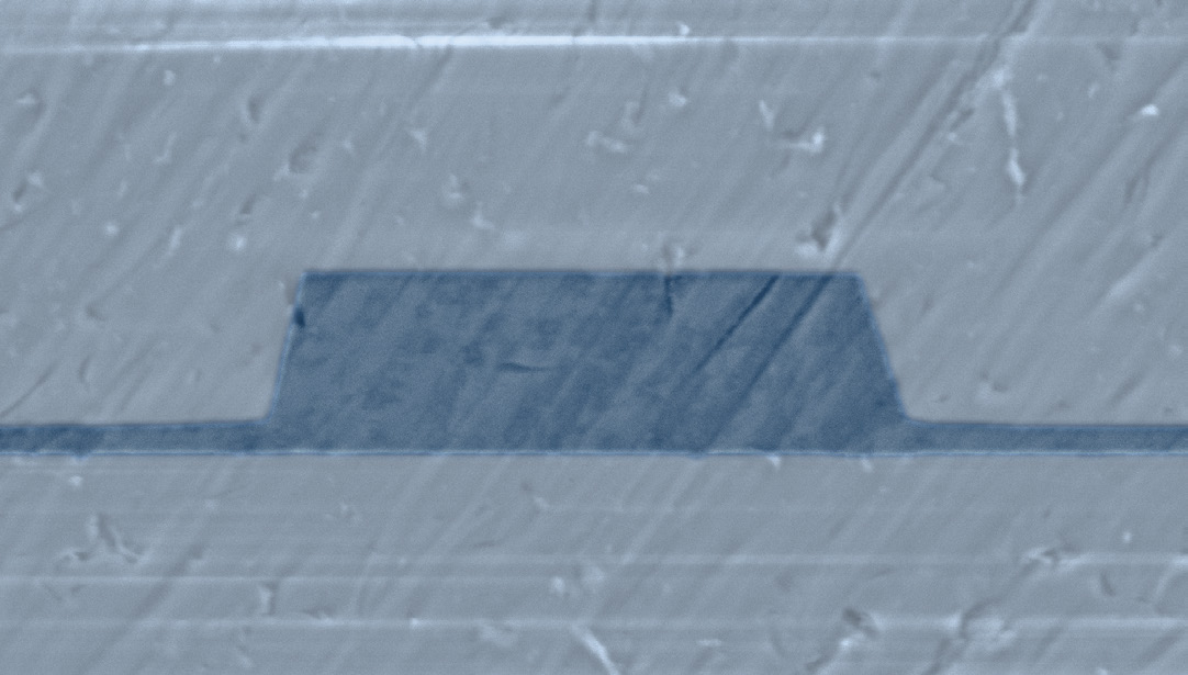
Fig 2: Second-harmonic generation in long periodically poled lithium tantalate waveguides. (a) Optical parametric fluorescence
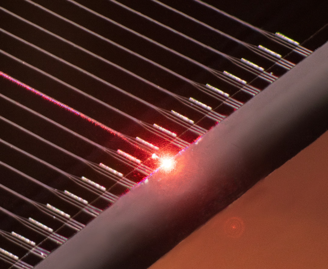
Fig 3 (page 3).
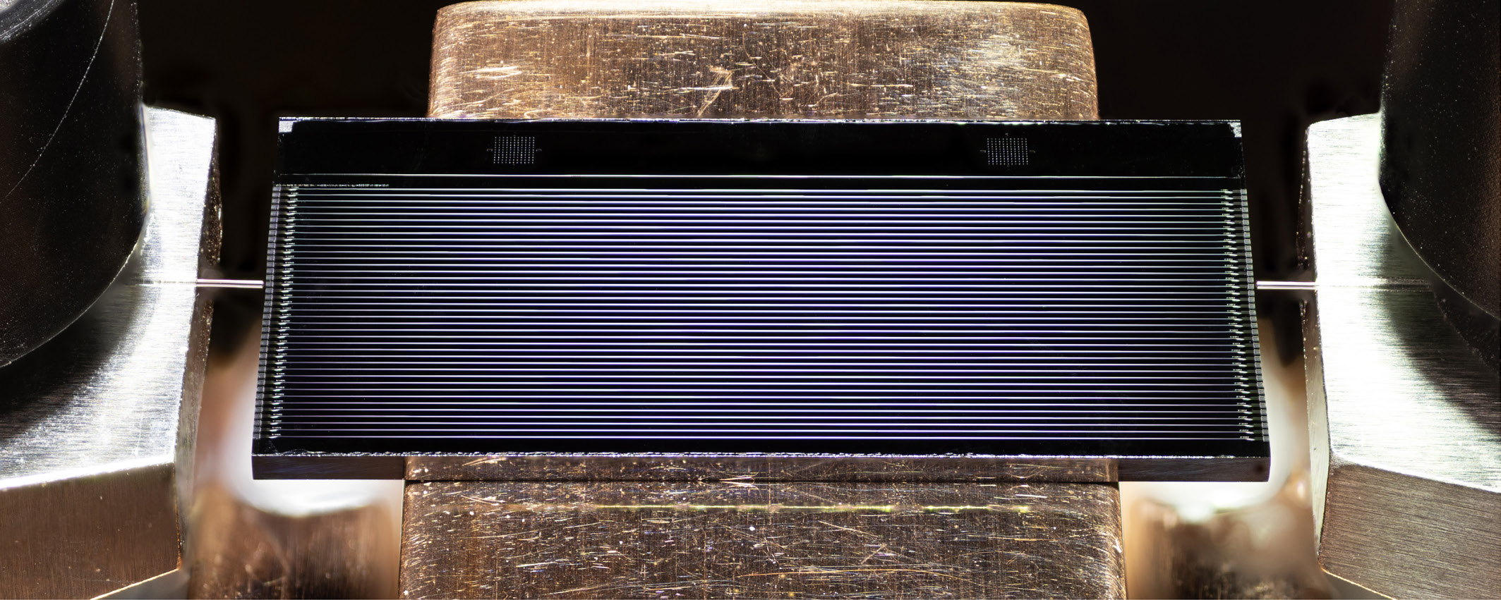
Fig 4 (page 3).

Fig 5 (page 3).
Fig 6 (page 3).

Fig 3: Measurements of broadband cascaded amplification in thin-film PPLT waveguides. (a) Single-frequency gain measurement.

Fig 8 (page 4).
Limitations
- Photorefractive effect and facet reflections cause gain fluctuations and limit pump power and output stability.
- Measured gain fluctuations due to coupling and polarization instabilities over broad spectral range.
- Maximum demonstrated on-chip pump power limited to ~2.3 W; higher powers might enable further gain but risk damage and instability.
- Fabrication tolerance requirements still present despite relaxed constraints; exact on-chip dispersion depends on nanoscale waveguide dimensions.
- No long-term aging or field deployment tests reported to assess reliability and environmental robustness.
Open questions / follow-ons
- How to further suppress photorefractive effects and facet reflections for improved operational stability at higher powers?
- Can even longer PPLT waveguides be fabricated with uniform periodic poling to boost gain at lower pump powers?
- What are the noise and nonlinear distortion characteristics under modulated signal conditions beyond CW testing?
- How scalable is the approach for full multi-channel telecom systems supporting WDM over hundreds of channels?
Why it matters for bot defense
For bot-defense and CAPTCHA practitioners focusing on optical communication security or hardware authentication leveraging optical signatures, this work provides a transformative broadband photonic amplification platform. The demonstrated ultra-wide gain bandwidth and all-optical modulation transfer capabilities indicate that integrated photonic circuits based on PPLT can enable next-generation, tunable, and power-efficient optical links and frequency converters outside conventional EDFA windows.
Practitioners designing optical challenge-response systems or hardware fingerprinting methods could exploit the wide spectral range, high gain, and quantum-limited noise of these OPAs for more robust, broadband optical identification. Also, the cascading nonlinear processes may inspire new forms of optical signal transformations useful for physically unclonable functions or anti-spoofing at the photonic hardware layer. However, the current device instability at high power and lack of field testing are critical considerations before deployment in security-critical applications.
Cite
@article{arxiv2605_22704,
  title={ All-band photonic integrated optical parametric amplification },
  author={ Nikolai Kuznetsov and Zihan Li and Tobias J. Kippenberg },
  journal={arXiv preprint arXiv:2605.22704},
  year={ 2026 },
  url={https://arxiv.org/abs/2605.22704}
}